Home > News > Industry News > From Crystal to Chip: The Fab Wafer Journey and Why Precision Cutting Matters
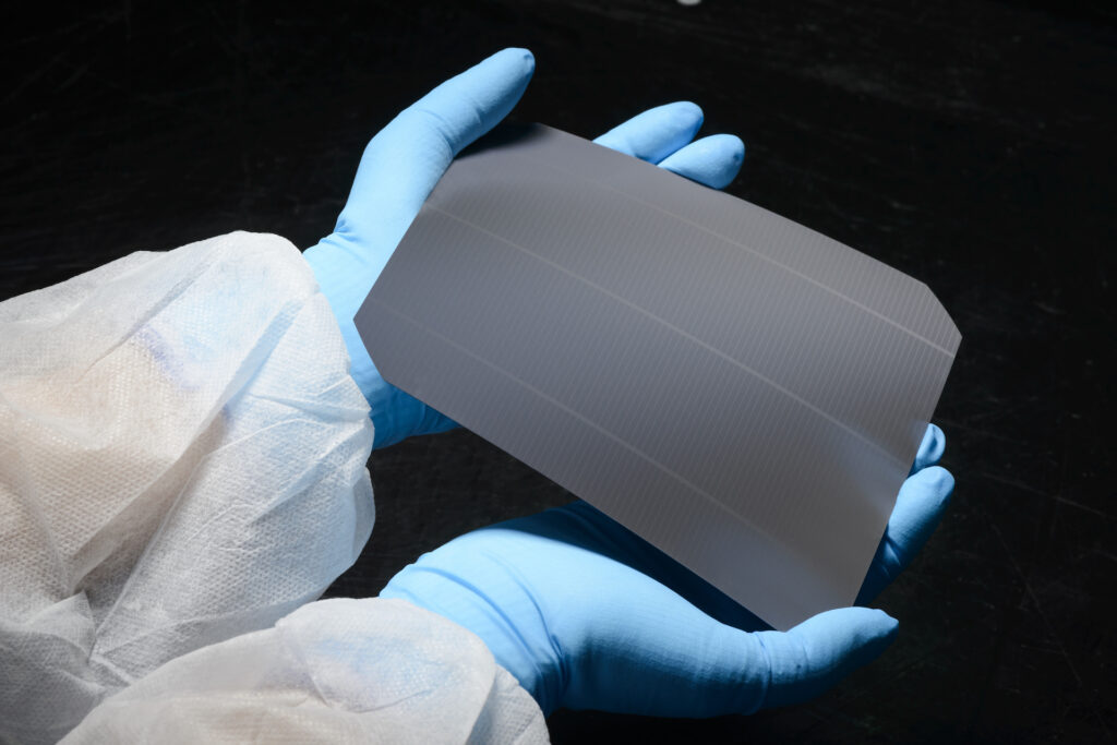
A fab wafer is a 200 mm or 300 mm disk of 99.999999999%-pure silicon sliced from a Czochralski-grown ingot — and the slicing step sets the ceiling for every chip that follows. Kerf loss wastes crystal, sub-surface cracks expand during high-temperature fab cycles, and thickness variation breaks photolithography focus. Endless diamond wire slicing addresses all three: kerf near 0.2 mm, minimal sub-surface damage, uniform thickness across the full wafer.
Wafer metrics (TTV, bow, Ra) · sand-to-wafer journey · inside the fab · why the cut defines yield.
Every chip begins as a fab wafer: a mirror-like disk of silicon, typically 200 mm or 300 mm in diameter, sliced from a crystal ingot that took days to grow. The quality of that slice propagates through hundreds of subsequent process steps — which is why precision cutting technology matters more than its share of the process chain suggests.
Silicon dominates wafer production for four reasons: it is abundant (refined from ordinary quartz sand), it has ideal semiconductor properties, it forms a stable oxide layer essential for transistors, and decades of development have made its manufacturing extremely mature.
The purity requirement is extreme: semiconductor-grade silicon must reach 99.999999999% — eleven nines. Among one billion silicon atoms, at most one may be an impurity, because a single stray atom in the wrong place can destroy a transistor.
| Metric | What It Measures | Why It Matters |
|---|---|---|
| Total Thickness Variation (TTV) | Thickness change across the wafer | Focus uniformity in photolithography |
| Bow and warp | Flatness deviation | Automated handling, layer alignment |
| Surface roughness (Ra) | Surface texture, in nanometers | Polishing cost, device performance |
| Sub-surface damage | Hidden micro-cracks below the surface | Wafer breakage during high-temp cycles |
High-temperature chemical reactions strip oxygen from silicon dioxide (sand), yielding metallurgical-grade silicon. Distillation and vapor deposition then purify it to electronic-grade polysilicon at eleven-nines purity.
Polysilicon melts in a quartz crucible above 1,400 °C. A seed crystal is dipped into the melt and slowly pulled upward while rotating (the Czochralski method), so silicon atoms solidify in the same crystalline orientation. A 300 mm ingot can exceed two meters, weigh hundreds of kilograms and take days to grow — any crystal defect can ruin large portions of it.
Slicing the ingot is among the most demanding steps in the chain. It requires extreme precision (consistent thickness across the full diameter), minimal kerf loss (every removed millimeter is grown-crystal money), and low sub-surface damage (no hidden cracks).
Edge grinding rounds the rim and adds the orientation notch; lapping flattens and removes saw marks; etching strips sub-surface damage; chemical mechanical polishing (CMP) creates an atomically smooth surface; final cleaning removes every particle. The finished wafer ships sealed to fabrication facilities.
A leading-edge fab can cost over $20 billion, with cleanrooms thousands of times cleaner than a hospital operating room. Once in production, a wafer passes through hundreds of steps: oxidation, photolithography, etching, ion implantation, deposition and metallization — repeated across 10–15 metal layers. Each chip is then tested; good dies are cut apart and packaged.
Thickness variation complicates photolithography and etching. Surface damage forces over-polishing, wasting silicon that took days to grow. Micro-cracks from unstable cutting expand during high-temperature fab cycles and turn promising wafers into scrap. Rough edges shed particles that contaminate cleanrooms and can ruin neighboring chips. Where a single yield point means millions of dollars, the cut is a value-defining operation.
This is why the endless diamond wire has become the preferred slicing solution: the loop moves in one uninterrupted direction, eliminating the reversals that cause surface irregularities, while embedded diamond abrasive removes material consistently from start to finish. The narrow kerf wastes less silicon, low sub-surface damage preserves usable thickness, and smoother as-cut surfaces need less polishing — directly translating into more wafers per ingot and lower cost per die.
See the process in action: diamond wire wafer slicing (YouTube).
From common sand to a flawless crystalline disk, the wafer journey demands extraordinary control over purity, structure and geometry — and the moment a massive ingot becomes thin wafers is where quality is locked in. For fabs that need to validate cutting performance on their own crystal, our free trial cutting service returns sliced samples with a full parameter report (WhatsApp +86-19937798228).
Related: Endless diamond wire for PV & semiconductor wafering · SiC wafer production with diamond wire saws · Custom endless diamond wire loops
If you have any question, please contact us